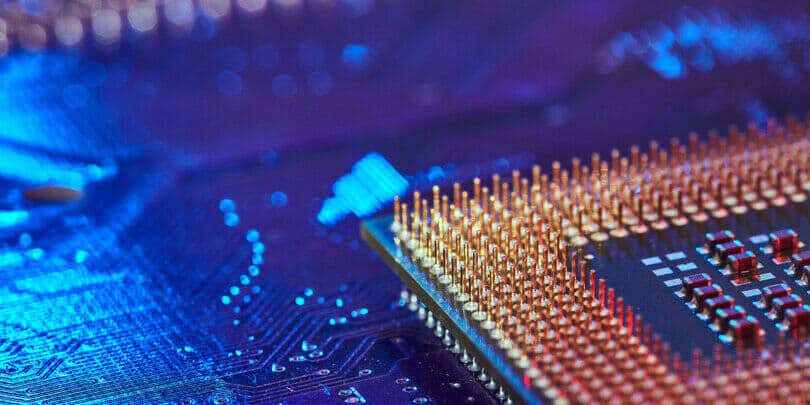
The semiconductor industry demands precision, innovation, and relentless efficiency. As…
Semiconductor Processing Equipment And Processes
While there seems to be an ongoing global chip shortage, the semiconductor market for consumer electronics is not showing signs of slowing down. Estimates show that the global market growth of the semiconductor industry is expected to hit USD 1,033 billion by 2031. This shows that there are great opportunities for semiconductor manufacturers that specialise in applied materials and know how to manage their supply chain well.
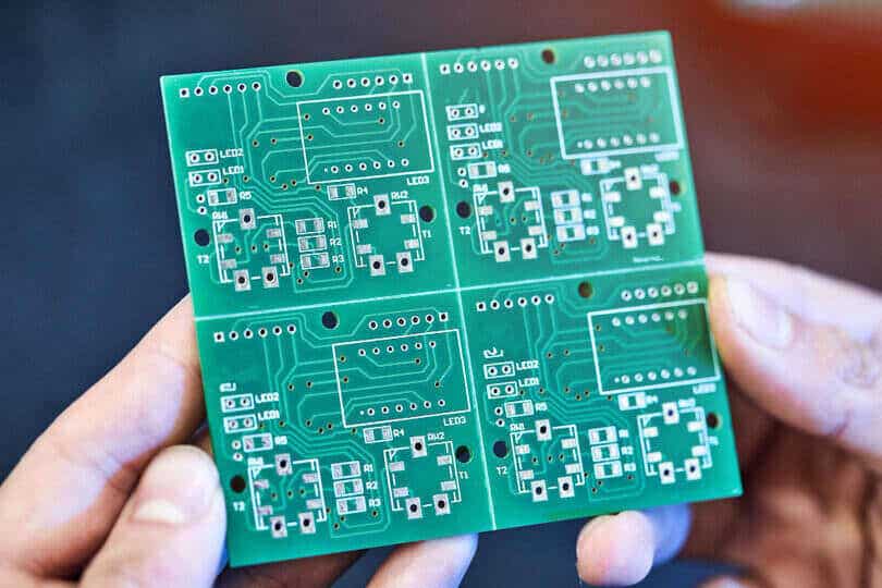
The semiconductor industry has been one of the most important industries in the world for the past few decades. Semiconductor chips are used in everything from cell phones to computers to cars. As demand for these chips has grown, so is the need for manufacturing companies to produce them more quickly and efficiently.
In this blog post, we’ll take a look at some of the latest machine tools used in semiconductor manufacturing and how they can be protected from wear and tear.
The Trend in Manufacturing Semiconductors
The first machines used in the semiconductor industry were simple manual lathes and milling machines. These machines were used to create the first semiconductor chips, which were made of silicon.
With the advent of digital technology, computer-controlled machine tools were developed that could create chips with widths measured in nanometers. Today, there are many different types of metrology equipment and machine tools used in semiconductor manufacturing, each with its own specific purpose.
Here are the new trends in semiconductor fabrication equipment and processes:
Miniaturisation
One of the most important trends to be aware of is the shift towards miniaturisation. As semiconductor devices get smaller, the mistakes that can damage them become more costly. You need to take extra care when handling and transporting semiconductor wafers, as even a small mistake can result in an irreparable loss. In addition, advances in technology have made it possible to pack more components onto smaller chips, which means that each individual component is even more valuable.
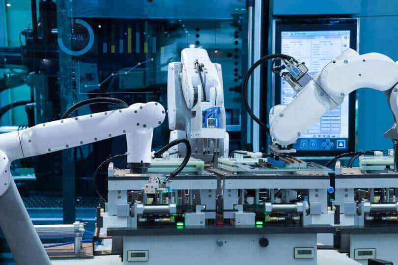
Automation
Another trend to be aware of is the increasing degree of automation in semiconductor fabrication facilities. While this can lead to increased efficiency and productivity, it also means that there are fewer people on the factory floor exposed to potential hazards.
Micro-enclosures
One trend that has been picking up steam in recent years is the use of micro-enclosures. Micro-enclosures are small, cleanrooms-within-cleanrooms that house critical semiconductor processing equipment. By isolating this equipment from the rest of the cleanroom, you can reduce the amount of particulate matter in your tools and products.
HEPA filters
Another trend that has been gaining traction is the use of HEPA filters in semiconductor processing equipment. HEPA filters are designed to remove 99.97% of airborne particles that are 0.3 microns or larger from a given air stream. By using HEPA filters in your semiconductor processing equipment, you can ensure that the air passing through your equipment is as clean as possible, which will help reduce particle contamination.
How Semiconductors Are Manufactured
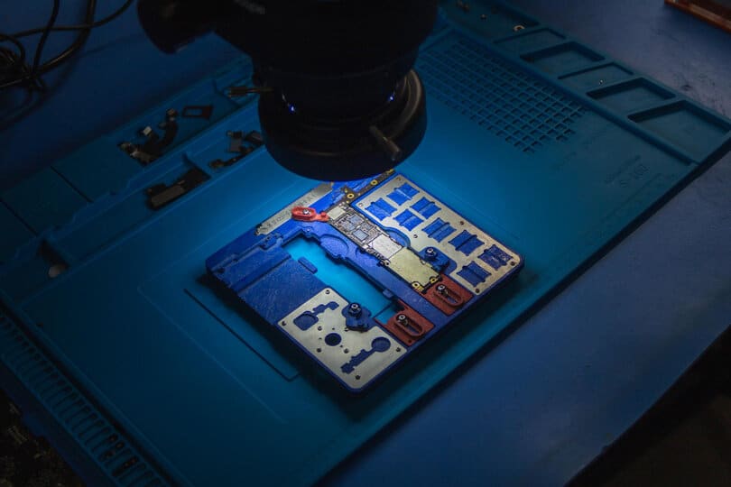
The first step in the semiconductor manufacturing process is creating silicon wafers. These wafers are what everything will be built on and need to be incredibly smooth and have few defects. The most common way to create these wafers is called the Czochralski Process. In this method, a small seed crystal of silicon is dipped into a molten pool of silicon. The crystal is slowly pulled out and rotated so that a large boule or cylindrical ingot of single-crystal silicon forms. Once the ingot has cooled, it’s cut into thin disks or wafers.
Now that the wafers have been created, they need to have circuitry patterns printed on them. This process is called photolithography and uses light to print the desired pattern onto the wafer.
First, the wafer is coated with a light-sensitive material called photoresist. Then, a mask (which is basically a stencil of the desired pattern) is placed over the wafer and both are exposed to ultraviolet light. The photoresist that isn’t blocked by the mask becomes harder while the exposed photoresist becomes softer. Next, the mask is removed and the now-hardened photoresist acts as an etch-resistant barrier during the next step in the process.
Once the circuitry patterns have been printed onto the wafer, it’s time to start building up layers of materials on top of it using chemical vapour deposition (CVD). CVD creates a film of material on top of the wafer by breaking down gases and depositing their molecules onto its surface in a very controlled environment. This allows for highly consistent films with few defects to be created. After each layer has been deposited, more photolithography takes place to pattern each new layer until all of the necessary layers have been built up.
The final step in this process is called etching where unwanted material is removed from between the different layers using either wet chemical etching or plasma etching. Wet chemical etching uses strong acids or bases whereas plasma etching uses ionised gas—or plasma—to remove material.
Once all of the unwanted material has been etched away, you’re left with your finished product: a completed semiconductor chip ready to be used in all sorts of electronic devices!
Types of Semiconductor Fabrication Equipment
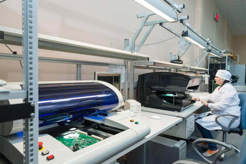
Here are the most important machines used in the production of semiconductors:
Lithography machine
One of the most important machine tools used in semiconductor manufacturing is the lithography machine. This machine is used to print circuit patterns onto silicon wafers. The circuit patterns are created using a mask, which is a template that contains the desired pattern. The lithography machine projects light through the mask and onto the silicon wafer, which etches the pattern into the wafer.
Deposition tool
Another important machine tool used in semiconductor manufacturing is the deposition tool. This machine is used to deposit thin films onto silicon wafers. Thin films are layers of material that are deposited onto a substrate using a variety of methods, such as chemical vapour deposition or sputtering. Deposition tools are used to create various types of thin films, such as conducting films, dielectric films, and photoresist films.
The most common type of deposition system is an ALD (atomic layer deposition) system. ALD systems work by alternately exposing the wafer to two different chemicals. The first chemical reacts with the surface of the wafer, and the second chemical reacts with the first chemical that was deposited on the surface of the wafer. This process is repeated until the desired thickness is achieved.
CVD (chemical vapour deposition) systems are another type of deposition system that is used in the semiconductor industry. CVD systems work by introducing a reactive gas into a chamber where it reacts with a solid substrate to form a thin film on the surface of that substrate. CVD systems can be used to deposit a wide variety of materials, including metals, dielectrics, and organic materials.
Dry etchers
Dry etchers are used in removing material from the surface of a wafer. They work by bombarding the wafer with high-energy ions that remove material from the surface. Dry etchers can be either plasma or laser-based.
Plasma etchers use a reactive gas to create a plasma that bombards the wafer with ions. Laser etchers use a focused laser beam to remove material from the surface of the wafer. Both types of dry etchers are used in the semiconductor industry today.
Sputtering systems
Sputtering systems are similar to CVD systems in that they are used to deposit materials onto surfaces. Sputtering systems work by bombarding a target material with ions. These ions knock atoms off of the target material, which then travels through space and deposit onto the surface of a nearby substrate. Sputtering systems can be used to deposit metals, alloys, and dielectrics onto surfaces. Sputtering is also sometimes used for etching applications.
Dicing machines
One type of machine used in the semiconductor industry is the dicing machine. Dicing machines are used to cut semiconductor wafers into smaller pieces. They use a rotating blade to make clean, precise cuts. Dicing machines are extremely important because they allow manufacturers to create very small semiconductors.
Linear guide
Another type of machine tool used in the semiconductor industry is the linear guide. Linear guides are used to move semiconductor wafers during the manufacturing process. They provide a smooth, precise movement that helps to prevent damage to fragile wafers. Linear guides are essential for ensuring that semiconductors are manufactured correctly.
X-Ray mask alignment tool
An x-ray mask alignment tool is used to align photomasks during the lithography step of semiconductor manufacture. A photomask is a template used to transfer a circuit pattern onto a semiconductor wafer. To be effective, the photomask must be aligned very precisely with the wafer surface. The x-ray mask alignment tool uses high-energy x-rays to expose the circuit pattern on the photomask onto the wafer surface.
Protecting Semiconductor Machines with Bellows Cover
Semiconductor equipment is used in the manufacturing of electronic devices and semiconductor products. The equipment is expensive and sensitive, so it’s important for semiconductor companies to take steps to protect it from damage. One way to do this is by using bellows covers.
What Are Bellows Covers?
Bellows covers are flexible, dust-tight enclosures that are used to cover and protect semiconductor machines and other types of equipment. They are made of durable materials like PVC or polyurethane that can withstand high temperatures and harsh chemicals. Dust is a major problem in semiconductor processing, so bellows covers help keep the equipment clean and free of contamination.
How Do Bellows Covers Work?
Bellows covers work by creating a seal around the machine that they are covering. This seal keeps dust, dirt, and other contaminants out while still allowing the machine to operate properly. The covers are also equipped with zippers or Velcro closures so that they can be opened and closed easily when needed.
Why Use Bellows Covers?
Bellows covers are an effective way to protect semiconductor processing equipment from damage. They help extend the life of the equipment by preventing dust and other contaminants from coming into contact with it. In addition, bellows covers can also help improve the quality of the product by reducing the amount of time needed for cleaning and maintenance.
Bellows covers can protect your semiconductor processing equipment from dust and debris. Dust particles can damage semiconductor machines and cause them to malfunction. Debris can also get caught in the machinery and cause problems. By fitting your equipment with bellows covers, you can keep it clean and running smoothly.
Another advantage of bellows covers is that they can protect your semiconductor processing equipment from environmental hazards. If you live in an area with a lot of insects or animals, for example, you’ll want to make sure that your equipment is covered so that creatures don’t get inside and cause problems. Bellows can also help protect against extreme weather conditions like wind, rain, and snow.
OTEGO – Providing Bellows Cover For Semicon Machines
Protecting your machine is more than just a matter of protecting its exterior. As protective covers are frequently exposed to harsh environments, it’s important that you choose the right material for best results. This will extend their lifetime and maximise performance!
OTEGO is a world leader in coating and laminating technologies. We export to more than 110 countries around the globe, counting local representatives on 5 continents! Our goal at OTEGO is to satisfy clients by delivering top-quality products with innovative features that meet their needs. This is why semiconductor equipment companies and other industries continue to trust OTEGO products for years.
The semiconductor manufacturing equipment market is growing and we’re positioned to take advantage of its growth with our technical textile products. Our coated fabrics are specifically designed to meet the needs of flexible bellow covers. With superior performance in both wet and dry environments, our materials provide operators with optimal control over their equipment while maintaining safety standards at all times through multiple thicknesses that can be welded/glued, or stitched.
We have seam sealing tapes, release liners, fabrics for exhaust management systems, and bellows covers. If you’re interested in our bellows cover or any of our products, feel free to contact us.
Related Posts